PCBE viewer
sweet_baked_pie
5,000+
downloads
Free
AppRecs review analysis
AppRecs rating 1.8. Trustworthiness 75 out of 100. Review manipulation risk 22 out of 100. Based on a review sample analyzed.
★☆☆☆☆
1.8
AppRecs Rating
Ratings breakdown
5 star
0%
4 star
0%
3 star
0%
2 star
100%
1 star
0%
What to know
✓
Low review manipulation risk
22% review manipulation risk
✓
Credible reviews
75% trustworthiness score from analyzed reviews
⚠
Mixed user feedback
Average 2.0★ rating suggests room for improvement
About PCBE viewer
A viewer specialized in PCBE which is a PWB editor. For check before ordering.
FEATURES
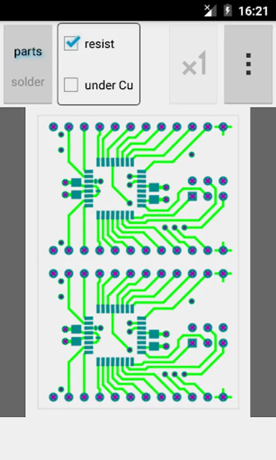
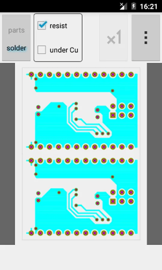
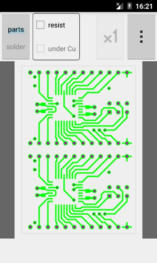
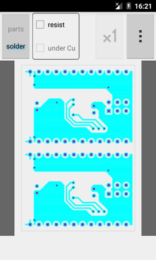
- 4 view types (parts/solder side, with/without resist).
- For check the footprint of SMD put on the screen at full scale.
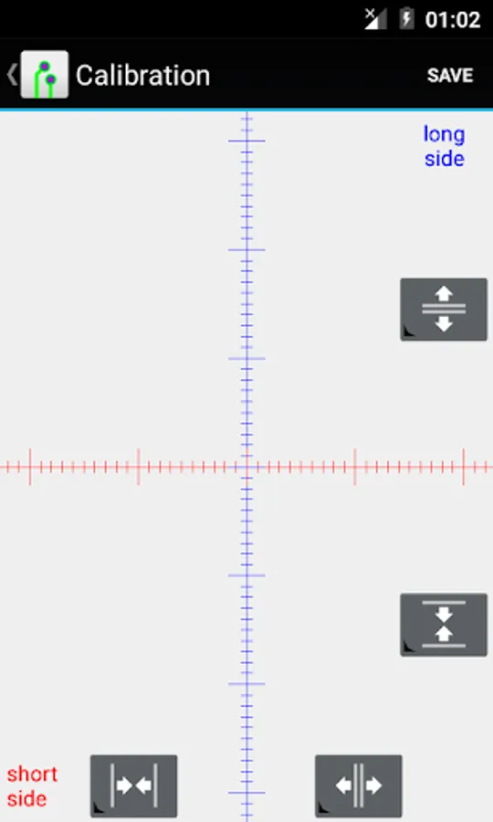
- Calibration of the screen width/height independently.
- Count the numbers of outlines/Vcuts/holes.
HOW TO START
- This app has no filer. Please start from your filer.
- The filename extension is .pcb.
SUPPORTED LAYERS
- L1:pattern on solder side (and L3)
- L2:pattern on parts side (and L10)
- L4:silk screen on parts side
- L5:resist on solder side
- L6:resist on parts side
- L7:outlines
- L8:holes
- (L11:Vcut)
Other layers are ignored.
TH (through hole) / NTH (drilled hole)
- The round hole on L8 is handled as TH when there are round or square pads on both L1 and L2 which have the same center.
- Otherwide, it is handled as NTH.
- However, the merged pads on L3/L10 are excluded from this rule.
NOTES
- All views are looked from parts side.
- Board size is max 22x22cm.
- Please do not use many periods(.) for file/folder name.
- PCBE is Mr.T.Takatoya's free software.
FEATURES
- 4 view types (parts/solder side, with/without resist).
- For check the footprint of SMD put on the screen at full scale.
- Calibration of the screen width/height independently.
- Count the numbers of outlines/Vcuts/holes.
HOW TO START
- This app has no filer. Please start from your filer.
- The filename extension is .pcb.
SUPPORTED LAYERS
- L1:pattern on solder side (and L3)
- L2:pattern on parts side (and L10)
- L4:silk screen on parts side
- L5:resist on solder side
- L6:resist on parts side
- L7:outlines
- L8:holes
- (L11:Vcut)
Other layers are ignored.
TH (through hole) / NTH (drilled hole)
- The round hole on L8 is handled as TH when there are round or square pads on both L1 and L2 which have the same center.
- Otherwide, it is handled as NTH.
- However, the merged pads on L3/L10 are excluded from this rule.
NOTES
- All views are looked from parts side.
- Board size is max 22x22cm.
- Please do not use many periods(.) for file/folder name.
- PCBE is Mr.T.Takatoya's free software.